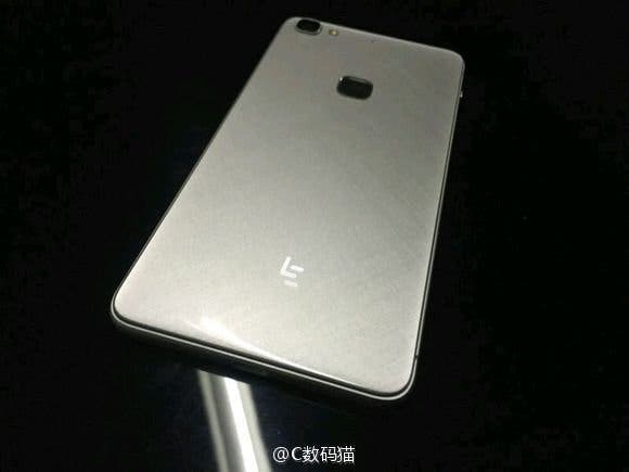
Benchmarks for the up coming LeTV LeEco 2 have emerged today and strangely they show the phone running a Mediatek Helio X25 chipset.
If you have been keeping your eyes on the latest chipsets from Mediatek, then you will know that the X25, an updated version of the X20, was meant to be a Meizu only exclusive chipset, but that doesn’t seem to be the case anymore.
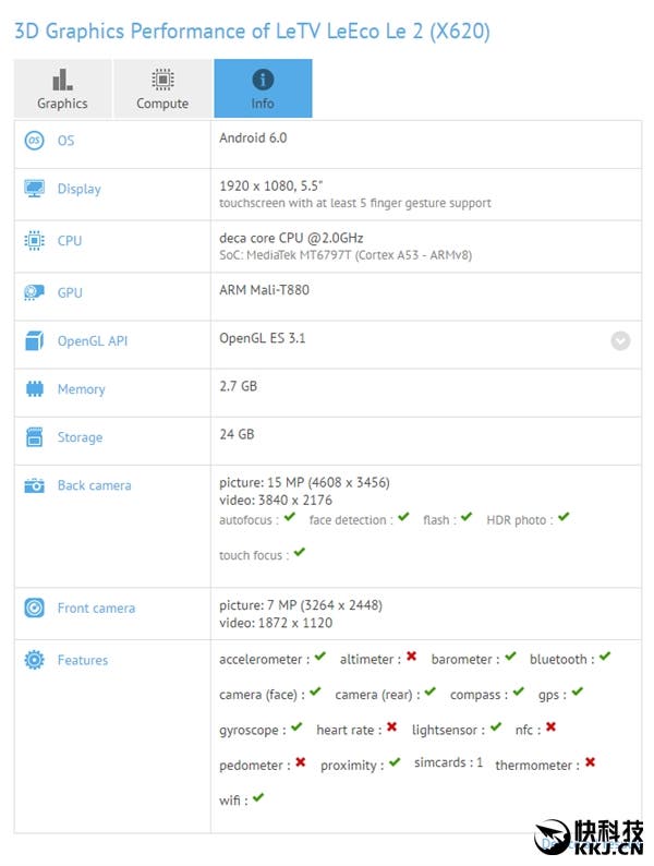
New benchmarks reveal that the LeEco 2 will also run a version of the Helio X25 (or Mediatek MT6797T) running at 2.0Ghz with 3GB RAM and 32GB memory (24GB left for users).
Gizchina News of the week
The specs also real that the latest LeTV phone will continue to use a 5.5-inch 1920 x 1080 display, but will see an update in the camera and OS departments. The benchmarks show the phone with Android 6.0, 15 mega-pixel rear camera, and 7 mega pixel front (likely an 8 mega-pixel front and 16 mega-pixel rear once the phone launches).
In addition to the Mediatek powered variant of the LeEco 2 a Snapdragon 820 model will also be launched with a higher price.
Both phones are set to be unveiled next month, so keep your eyes on GizChina for the latest.


I’m pretty certain the x25 runs at 2.5ghz and not 2.
Most likely this is not the final software build, or that geekbench mistook the X20 for the X25(happens with new SoC’s sometimes)
That was my thought too. Seems like this is actually the X20 and not the X25.
I wonder if this is a half way house between the x20 and x25, maybe only the GPU is clocked faster on this. There is also the possibility that this won’t be released for another 3-4 months by which time Meizu’s exclusivity will have expired.
Apparently Sammy got hold of the X25 as well… http://www.gsmarena.com/galaxy_s7_with_helio_x20_and_x25_chipsets_spotted_in_benchmark-news-17476.php
I would highly doubt this, it makes no sense for Samsung. Geekbench has all sorts of phone/chip combinations that never see the light of day.
Never saw a Samsung with MTK chipset.
Turns out X25 is not so exclusive to Meizu as we have been led to believe.
I`m keeping a close eye on this device, certainly looks good for the price, only problem is that they are using the same Sony 230 sensor from their previous lineup to cut costs.
There’s no problem with that sensor if they use a good lens and properly optimize it. It takes stunning photos on the Meizu’s that use it.
The sensor itself is not bad, just dated, it has less than stellar low-light performance and is very good in macro shots and when there is plenty of light, but it`s not a real upgrade. I am a Flex 2 and Honor 7(which boasts the same sensor btw)user and I am looking for something better at that price point besides benchmarks.
Low light performance can vary from device to device with the same sensor based on the aperture, lens and software used. But I have yet to use a smartphone with good low light performance, (even the ones just released) the sensors are just too small. A newer sensor with the same old lens and poor optimization will gave similar results.
Price? I don’t see where they mentioned the actual price on the phone.
didnt the meizu thing say it would be exclusive to them for a time?
Yes, but it seems that LeTv offered good money to MTK to give them access to the chip also.
money does talk
Or Meizu has exclusive rights for a set period of time. There is still so little known about this and Meizu’s plans. This might not be launched for months.
And of course no sdcard and non removeable battery…
As long as it has quick charge non removable battery really isn’t needed.
But you know you don’t have a wallet charger in your pocket and not always you have an easy access to one. I mean that the new phones must last through the day without even the need to think about the battery, but still that’s not the case
I also don’t have extra batteries in my pockets. The last three new phones I had all lasted at least a day, some even longer.
I’m pretty certain the x25 runs at 2.5ghz and not 2.
Most likely this is not the final software build, or that geekbench mistook the X20 for the X25(happens with new SoC’s sometimes)
That was my thought too. Seems like this is actually the X20 and not the X25.
I wonder if this is a half way house between the x20 and x25, maybe only the GPU is clocked faster on this. There is also the possibility that this won’t be released for another 3-4 months by which time Meizu’s exclusivity will have expired.
Apparently Sammy got hold of the X25 as well… http://www.gsmarena.com/galaxy_s7_with_helio_x20_and_x25_chipsets_spotted_in_benchmark-news-17476.php
I would highly doubt this, it makes no sense for Samsung. Geekbench has all sorts of phone/chip combinations that never see the light of day.
Never saw a Samsung with MTK chipset.
Oh man , this one would be perfect with micro sd card slot ,or at least a version with 64gb
Turns out X25 is not so exclusive to Meizu as we have been led to believe.
I`m keeping a close eye on this device, certainly looks good for the price, only problem is that they are using the same Sony 230 sensor from their previous lineup to cut costs.
There’s no problem with that sensor if they use a good lens and properly optimize it. It takes stunning photos on the Meizu’s that use it.
The sensor itself is not bad, just dated, it has less than stellar low-light performance and is very good in macro shots and when there is plenty of light, but it`s not a real upgrade. I am a Flex 2 and Honor 7(which boasts the same sensor btw)user and I am looking for something better at that price point besides benchmarks.
Low light performance can vary from device to device with the same sensor based on the aperture, lens and software used. But I have yet to use a smartphone with good low light performance, (even the ones just released) the sensors are just too small. A newer sensor with the same old lens and poor optimization will gave similar results.
Price? I don’t see where they mentioned the actual price on the phone.
didnt the meizu thing say it would be exclusive to them for a time?
Yes, but it seems that LeTv offered good money to MTK to give them access to the chip also.
money does talk
Or Meizu has exclusive rights for a set period of time. There is still so little known about this and Meizu’s plans. This might not be launched for months.
3 phones Andy, there is a SD652 LeEco x520 too.
please LE eco
And of course no sdcard and non removeable battery…
As long as it has quick charge non removable battery really isn’t needed.
But you know you don’t have a wallet charger in your pocket and not always you have an easy access to one. I mean that the new phones must last through the day without even the need to think about the battery, but still that’s not the case
I also don’t have extra batteries in my pockets. The last three new phones I had all lasted at least a day, some even longer.
Oh man , this one would be perfect with micro sd card slot ,or at least a version with 64gb
Don’t care a bit how powerful is this phone if they’re planning to ruin all with the last sentence: ” Battery 3000mah”
What happened with the Le Max Pro? (the supposed fisrt 820 smarthphone)
They only shows the phone in the CES?
3 phones Andy, there is a SD652 LeEco x520 too.
please LE eco
The GPU is worse than the Adreno 418 of the Mi4c. Why would I want this over a 650 or 652 powered device?
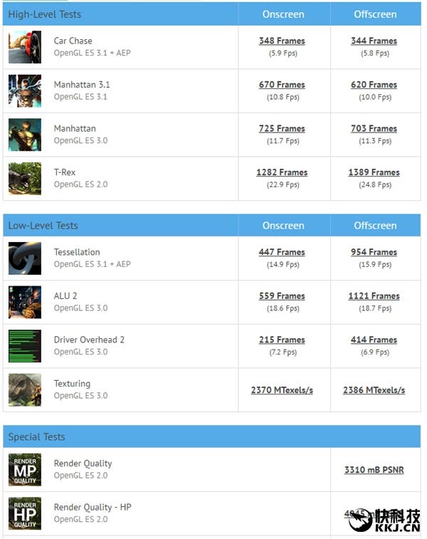
Meizu Pro 6’s results disagree with your statement. Probably it has been tested while running at some kind of power saving mode. 60% difference at T-Rex and Manhattan can’t be explained with slightly lower clock speed of exact same GPU. Strangely other results are close enough.
Besides than having more powerful both CPU and GPU, 20nm vs 28nm nodes should be enough answer comparison to the SD650 and SD652. Not to mention lack of power hog Cortex-A57 cores of the SD808.
First the results for Meizu MX6 Pro are fake, secondly Mali T880 @ 850 MHz should be as fast as Adreno 510 but it will consume 170% energy of Adreno, third their is a very small difference between consumption of TSMC HPL 28nm & regular 20 nm PL. Other than that S65x series come with better multimedia capabilities (mostly still not utilized) & better cellular radio.
Sorry, but it isn’t fake. GFXBench database are a reliable source. It’s pretty much same with Le 2’s results except Manhattan and T-Rex benchs. Also comparing to Kirin 950 you should see that it pretty much close again including Manhattan and T-Rex. Something clearly is different at Le 2’s Manhattan and T-Rex benchmarks.
Nobody has released power consumption of either GPU. It’s possible to estimate X25’s based on Kirin 950’s (again) estimated power consumption figure (which is released at Anandtech) via TSMC 20nm vs 16nm FinFET power consumption figures. According to the TSMC 20nm consumes 25% less power than 28nm BTW.
As far as I know nobody bothered yet releasing even Adreno 530’s power consumption figures let alone Adreno 510. Nobody bothers to do that for mid range chips anyway.
It is fake as the score is abnormally higher compared to both Kirin 950 (@ 50 MHz more & 35% bigger RAM bandwidth) & other X25 scores.
How about your “reliable surce” & comparation of Mate 8 to the Samsung Galaxy A9, even A9 have a larger display they have similar size of battery & don’t forget Kirin 950 is more powerful effects than X25.
https://gfxbench.com/compare.jsp?benchmark=gfx40&did1=27447856&os1=Android&api1=gl&hwtype1=GPU&hwname1=Qualcomm+Adreno+%28TM%29+510&D2=Huawei+Mate+8+%28NXT-xxx%29
As there are a run time data for TRex you can clearly see that power estimations I told are there.
Honey there is much more than just a nm for used process to take into consideration; there is a rooting lib lv, inter blocks & cetera. When I say there is a little difference between bulk not future optimized 20 nm planar to the high optimized hi performance 28 nm of same TSMC I ment that as a fact. You can find estimations on that site for 20 nm Samsung planar & you will see how achieved results are on pair with 28nm HPL to the 28nm PL.
So only thing you need to do is a little reading along with putting some thinking in the use.
It isn’t abnormally higher compared to Kirin 950. Despite your claim Le 2’s results is on the same level at Car Chase, Manhattan 3.1, Tessellation, ALU 2, and Texturing. At Manhattan and T-Rex Le 2’s results are abnormally low.
Moreover Le 2’s results except Manhattan and T-Rex is also on the same level with Mate 8. That’s where your claim failed you.
Obviously you don’t know meaning of fake. Benchmarked devices performed those results, period. Sweetheart, you should have said that cheated. It undeniably tested with MT6797 and performed that results regardless of other considerations.
Mate 8 vs Galaxy A9 comparison doesn’t provide power consumption data. Sweetheart, didn’t you know battery life depends on a lot of factors including biggest power hog of the system which is screen. Screen size is also irrelevant. Even different kind of LCD power consumptions varies greatly not to mention AMOLED has huge advantage at that kind of content. What about peek brightness? Moreover even if it was a offscreen test results you can’t take it as GPU vs GPU power consumption. I’m not over yet sweetheart, power drain also depends on battery properties like output and temperature.
Now, can you explain how you reached that certain 70% figure sweetheart?
Anandtech actually did a test and proved that 20nm is considerably more efficient than 28nm. Period.
http://www.anandtech.com/show/8718/the-samsung-galaxy-note-4-exynos-review/2
You always making bold statements with never providing any data or proper source. Except you, nobody making such a bold statements at nowhere, without providing measurements from actual tests or providind data from manufacturers. You are probably the first and last person ever claiming Adreno 510 has been most power efficient mobile GPU as well I know. Though despite you habits without data I can’t say otherwise, that claim smells like utter BS to me. Even if we assume that its architechture is superior to all competing architechtures and assuming it shares exact same architechture with Adreno 530, 16nm FinFET would be enough to make the latter most efficient one.
Admit it sweetheart, actual source of estimated power consumption of Adreno 510 and most efficient mobile GPU is no other than your eyes.
Quite: “All in all, the argument that this 20nm chip should be more power efficient than the competitors’ 28nm is not completely factual and doesn’t seem to hold up in practice. The process still seems young and unoptimized compared to what TSMC offers on 28nm”
Second paragraph at the end of the same page of the same article. I advise you to start thinking about waring eye glasses.
Now let’s assume how TSMC 20nm bulk (as they also never optimized it, instead they jumped to 16nm FinFET) is still a little better than Samsung’s that still doesn’t make it much better than 28nm HPM, as I actually claimed.
Their is a reason why I actually compared Mate 8 to the Galaxy A9 as they are closest match both with 4000 mAh battery even Mate have 6″ display vs 5.5″ on this A9 model, both are Amoled & are only ones with enough data to do a real comparation especially in battery test, by the way results displayed are based on mid scores of all runs so your argument about consistency & Lux on display don’t stand. People usually run tests with auto brightness so there shouldn’t be much difference by the way usual practice for pro testing is putting brightness to 200 nits. The T-Rex battery test difference of 47% more in favor of S652 or A510 if you like clearly speaks about much better power efficiency of A5xx generation. A530 is advertised as most powerful & most power efficient mobile GPU currently available on market which is true but as you won’t need all that power & it will consume much more battery then a scaled down litle brother A510 in most & every game as clocking logic is far from good. Simply A510 is a sweet spot for 1080p gaming & it does this task most power efficient, A530 is capable of pushing 2K even 4K but all of this eats to much of battery & on sub 7″ is useless as you won’t see extra details, VR is other pair of slippers but we are not there yet so I won’t touch this topic. Basicall & well known fact why the Adrenos are leader in performance per W are in the way they are designed as single cluster as single cluster scales 100% in performance & every additional adds around 68~75% depending how good design is.
Actuality T880 MP4 implementation on X25 got a greater performance hit than I anticipated in the first place & it’s every way worse & slower than A510 which is not by all means shining in the GFX bench.
https://gfxbench.com/compare.jsp?benchmark=gfx40&did1=31731956&os1=Android&api1=gl&hwtype1=GPU&hwname1=Qualcomm+Adreno+%28TM%29+510&D2=LeTV+LeEco+Le+2+%28X620%29
If you compare 3D Mark scores difference will become more significant.
It’s very hard to provide colorful evidence to blind people.
Now with all data & facts provided from me and none from you expect those that actually did go with my initial hypothesis I expect you at least to buy those eye glasses as it seams you need them, on the other hand I don’t expect to see you becoming any more intelligent as so far you failed badly to use your brains. Well at least you will see better.
Even as unoptimized 20nm process of Samsung beats 28nm Samsung easily. That sentence is about 20nm Samsung vs 28nm TSMC.
Both X20/X25 and SD650/652 manufacturing at TSMC. Hence that sentence about Samsung 20nm vs TSMC 28nm it can’t be applied to 20nm TSMC vs 28nm TSMC comparison.
Where do you get idea that unoptimized mean not better power consumption comparison to larger nodes?
What are you smokin? Sweetheart, I’m sorry but your logic failed you again.
Mate 8 has LCD screen not AMOLED. So you are builded your whole logic on a false assumption. Next time just Google it.
Do I need to repeat that? Mate 8 has LCD screen. Not to mention
Moreover you can’t assume all of those devices even most of them tested at auto brightness or setting at 200nits. Also autobrightness doesn’t necessarily mean same level brightness. You obviously have no idea what are you talking about.
I’m not over yet again sweetheart, Galaxy A9 beats Redmi Note 3 Pro too with much larger screen. I can imagine your face right now.
YOU-CAN’T-ESTIMATE-EVER-POWER-CONSUMPTION-OF-GPU-FROM-THAT-PARTICULAR-BENCHMARK-HENCE-THERE-IS-A-LOT-MORE-AFFECTS-POWER-DRAIN.
Actually Adreno 530 advertised as more efficient than previous generation, not as most power efficient. Stop making things up out of your eyes sweetheart.
http://www.qualcomm.com/media/documents/files/qualcomm-adreno-530-gpu-infographic.pdf
So you are builded your logic on a false assumption, again.
You are in neck deep logic fallacies and false assumptions. You are both arrogant and ignorant. When somebody disagree with you, you are making it personal. Worse in the process making yourself a clown.
Grow up.
Ok you are right about Mate display, still their is no better comparation currently available. Adreno 530 is advertised as more power efficient from previous generation that whose still more power efficient than T7, T8 Mali’s. Auto brightness is what it is. I told that professional benchmarkers set the brightness value to 200 nits, you again have troubles reading…
“Where do you get idea that unoptimized mean not better power consumption comparison to larger nodes?”
From officiall projections when they announced 20nm process compared to same ones of the 28nm HPM. In best case difference is about 4%.
“Both X20/X25 and SD650/652 manufacturing at TSMC. Hence that sentence about Samsung 20nm vs TSMC 28nm it can’t be applied to 20nm TSMC vs 28nm TSMC comparison.”
Actuality I did state how TSMC 20nm process is better & more advanced than Samsung’s I also stated how you won’t find a direct comparation of TSMC 20 nm to 28nm HPM earlier & I will again state how IT’S NOT SIGNIFICANT.
“YOU-CAN’T-ESTIMATE-EVER-POWER-CONSUMPTION-OF-GPU-FROM-THAT-PARTICULAR-BENCHMARK-HENCE-THERE-IS-A-LOT-MORE-AFFECTS-POWER-DRAIN”
THEIR IS NOTHING EFFECTING A POWER DRAIN MORE THAN GPU UTILIZATION!!! Besides Gxf is pretty little on CPU block, display is second largest consumer in this case. Certainly Samsungs UI & bunch of apps and frameworks in the background will case bigger power drain than none of those on Huawei along with EmotionUI that lacks even app drawer. I can’t do accurate projection but let’s say 35~40% is in self margins compared to so high clocked T880 MP4.
Make this in personal by finding either better comparation or some facts to any of your claims. So far I did present some not so good comparations but it’s still much better to none that you presented so far. Pardon my ignorance but you didn’t present anything that I could ignore. & stop with that faggat shit.
Just learn to stop when you proven wrong. Seriously, how old are you? Insulting won’t affect to outcome, ever. You are just getting lower and lower. Nobody will take you serious as a grown up, when you spitting out with rage. Grow up.
Again you are feeding this thread with false information.
I can provide a link from TSMC, officially they claim that 20nm offers 25% power saving.
I can provide a link showcases 20nm Samsung consumes 30% less power than its 28nm counterpart from actual power measurements.
Can you provide us a link from official sources shows that difference is just 4% AT BEST? I can even accept an unofficial source if it presented with results of a proper test.
Did I miss your explanation of how Galaxy A9 did outlast by 10% Redmi Note 3 Pro with the exact same GPU with even 19% larger display? You are just clinging to straws.
I’m still waiting for your explanation of Adreno 510’s being 70% more efficient STORY. You must have a solid calculation.
GPU power drain also varies greatly depending on GPU just like screens. Considering budget phones frequently pairing weak GPUs with cheap (means power hungry) LCDs I can safely say you are out of your depth again. Basically it depends on GPU and screen pair.
Moreover it was never my point. I said that power drain depends on other factors. Screen is just one of a long list.
“Just learn to stop when you proven wrong.” talking to your self aren’t you? I am older than you. I didn’t called you a honey, sweetheart, sauger so if that someone after that tells you to stop with faggat stuff & that insult you then you probably have problems…
I never claimed how it’s 70% more efficient I claimed 35~40%.
You can stick your link where sun don’t shine.
Here you go a link with a little more detailed power/performance/power savings technics, proces optimizations inter blocks & cetera along with their additional dependences when combined together. It’s still not in depth. If you want I have deeper wite paper for 28nm FD-SOI?
https://www.synopsys.com/Company/Publications/SynopsysInsight/Pages/Art4-low-power-IssQ2-12.aspx?cmp=Insight-I2-2012-Art4
By the way 28nm HPM is 40% more power efficient than 28nm HP, 20nm is HP & it’s compared to HP as TSMC always do. Now this would actually suggest how 28nm HPM is more efficient than 20 nm HP which is not entirely true if you take into consideration & SRAM (which eats a large die size) along with density, they probably cost approximately the same now. So at the end it seams how actually 28nm HPM culd actually be around 4~5% better in terms of power consumption. Qualcomm learned a hard way how 20nm HP is not an improvement over 28nm HPM on last year S810.
Actuality I did proven that: A510 is more efficient than T880 MP4 @ 850 MHz, shown how it’s faster & showed how 28nm HPM is actually even better than 20 nm HP from TSMC. Those are the facts, we can argue about actual projections but ewen if we had actual & identical hardware like for instance this LeTV in both versions we still couldn’t make fully acute numbers out of them.
Now I actually have right to be pissed off as I whose wright all of the time wile you ware annoying litle crab. In the future don’t make a bold claims & hard headedly assume things without any real hard stand points. I know also to behave quite nice when I am a pouched nicely or at least normally with a normal question.
Before reading rest of your whole new rant, I have to say you are obviously a liar. Simple as that.
“I didn’t called you a honey”
As a matter of fact, you did. Without provocation. You are a liar. That’s a fact too. Your post is still there.
“Honey there is much more than just a nm”
“I never claimed how it’s 70% more efficient I claimed 35~40%.”
Seriously?
Well, actually you did that too. That post is there too. You make me laughed out loud, literally. How can you denied those?
“First the results for Meizu MX6 Pro are fake, secondly Mali T880 @ 850
MHz should be as fast as Adreno 510 but it will consume 170% energy of
Adreno,”
You caught liar. Again.
Your link doesn’t contain a single figure of the 20nm planar nodes power consumption comparison to 28nm. Nice try. I would gladly stick it to depths of my brain if it has a useful info on that matter.
I would like to have a 28nm FD-SOI vs 20nm planar comparison, if you are stupid enough to try to do that. I will enjoy to trash out it with pointing out that 28nm FD-SOI are completely different than 28nm planar processes. Neither of those chips manufactured at FD-SOI. No mobile chip manufactured with it, ever.
It would be whole another story if Snapdragon 650/652 manufactured at 28nm FD-SOI. But it didn’t, period.
So we still don’t have where do you get that Adreno 510 is 70% more efficient than Mali-T880 MP4 claim.
We also don’t have where do you get that 20nm is 4% more efficient at best than 28nm claim. Other than an assumption over TSMC’s figure.
Actually your claim was 20nm was 4% more efficient at best. Now, you are claiming actually 28nm HPM is about 4-5% more efficient. What did change in a couple of hours?
Apple A8 was fine with at TSMC’s 20nm.
If Exynos 5433 is any indicator, just at CPU side power consumption of Snapdragon 810 can reach up to 8-9 watt. Which is crazy. Cortex-A57 clearly was a power hog. Even at 14nm FinFET it have caused throattling.
Snapdragon 652 at 20nm would be a threat to Snapdragon 820 and it would cost more. That’s why they dropped 20nm, not because of that the SD810 fiasco.
Insults and lies won’t change to the result. Grow up. Or don’t. It just humiliates you in public further and further. Spit out with rage, throw insults.
You really are dumb ass acting as a little kid.
If I stayed that T880 will consume 170% of the power of A510 is using that translates in to 40% efficiency, if I claimed 70% (& I didn’t) more power efficient that would mean it uses 30% power to achieve same performance as T880 or how T880 uses 320% power.
The Meizu MX6 Pro result is fake as not only that it scores more than any other X25 it scores more than HiSilicon Kirin 950 & that part is simply impossible.
TSMC 28nm process is very scalable, HPM is based on HP that is adapted to use less power & provide good performance. In the figure 2 of linked article their is a simple example how it’s possible to achieve additional power consumption cut (30% less leaking) on it. The part you simply aren’t able to get in your head is how TSMC’s 20nm process is simply not scalable nor adjustable (no one bothered to translate libs for abandoned process). At the base TSMC 28nm HPM & TSMC 20nm use same base voltage so they will consume relatively same power. How ever their is much more in to it from using specific inter blocks & how blocks are rutted & it’s possible to do this better on 28nm HPM than on 20nm as most of the tools are not available for the 20nm process. Qualcomm actually achieved same to better power consumption on HPM than LP back in the S800, S600 day’s. They are by far most experienced in using it. Me by the best example that is good documented how important rooting, placement & inter blocks is one tied to Samsung Exunos SoC’s with Cortex A15 as they achieved in 3 cycles to bet it’s power consumption down almost by 50% wile switching only from 28nm to 20nm. You’re own claim is how Samsung’s 20 nm is 30% more power efficient, the rewiev showed us differently & this power consumption of A15 is actually based on real measurements & not projections.
Take a look if you have time:
http://cyberparse.co.uk/2015/02/10/arm-a53a57t760-investigated-samsung-galaxy-note-4-exynos-review/
By the way this is much deeper analys then one you are referring at, actually one you are referring at is based on this & simplified.
Exunos 5433 managed to drove 7.11 Watt from a big cluster (±100 mW margin).
At the end TSMC is advertised it’s 28nm HPC+ process that consumes less power & costs less than 20nm wile delivering comparative performance of 20nm & 28nm HPM wile being compatible with 28nm HPM tools. So you see (I hope) it’s not all in nm, their is much more in implementation & it’s possible to achieve better implementation on 28nm. Even Samsung that actually did optimized it’s 20nm process along with tools and libs is abandoning it in favor of 14nm FinFET & 28nm FD-SOI.
Don’t care a bit how powerful is this phone if they’re planning to ruin all with the last sentence: ” Battery 3000mah”
What happened with the Le Max Pro? (the supposed fisrt 820 smarthphone)
They only shows the phone in the CES?
The GPU is worse than the Adreno 418 of the Mi4c. Why would I want this over a 650 or 652 powered device?
Meizu Pro 6’s results disagree with your statement. Probably it has been tested while running at some kind of power saving mode. 60% difference at T-Rex and Manhattan can’t be explained with slightly lower clock speed of exact same GPU. Strangely other results are close enough.
Besides than having more powerful both CPU and GPU, 20nm vs 28nm nodes should be enough answer comparison to the SD650 and SD652. Not to mention lack of power hog Cortex-A57 cores of the SD808.
First the results for Meizu MX6 Pro are fake, secondly Mali T880 @ 850 MHz should be as fast as Adreno 510 but it will consume 170% energy of Adreno, third their is a very small difference between consumption of TSMC HPL 28nm & regular 20 nm PL. Other than that S65x series come with better multimedia capabilities (mostly still not utilized) & better cellular radio.
Sorry, but it isn’t fake. GFXBench database are a reliable source. It’s pretty much same with Le 2’s results except Manhattan and T-Rex benchs. Also comparing to Kirin 950 you should see that it pretty much close again including Manhattan and T-Rex. Something clearly is different at Le 2’s Manhattan and T-Rex benchmarks.
Nobody has released power consumption of either GPU. It’s possible to estimate X25’s based on Kirin 950’s (again) estimated power consumption figure (which is released at Anandtech) via TSMC 20nm vs 16nm FinFET power consumption figures. According to the TSMC 20nm consumes 25% less power than 28nm BTW.
As far as I know nobody bothered yet releasing even Adreno 530’s power consumption figures let alone Adreno 510. Nobody bothers to do that for mid range chips anyway.
It is fake as the score is abnormally higher compared to both Kirin 950 (@ 50 MHz more & 35% bigger RAM bandwidth) & other X25 scores.
How about your “reliable surce” & comparation of Mate 8 to the Samsung Galaxy A9, even A9 have a larger display they have similar size of battery & don’t forget Kirin 950 is more powerful effects than X25.
https://gfxbench.com/compare.jsp?benchmark=gfx40&did1=27447856&os1=Android&api1=gl&hwtype1=GPU&hwname1=Qualcomm+Adreno+%28TM%29+510&D2=Huawei+Mate+8+%28NXT-xxx%29
As there are a run time data for TRex you can clearly see that power estimations I told are there.
Honey there is much more than just a nm for used process to take into consideration; there is a rooting lib lv, inter blocks & cetera. When I say there is a little difference between bulk not future optimized 20 nm planar to the high optimized hi performance 28 nm of same TSMC I ment that as a fact. You can find estimations on that site for 20 nm Samsung planar & you will see how achieved results are on pair with 28nm HPL to the 28nm PL.
So only thing you need to do is a little reading along with putting some thinking in the use.
By the way mid range SoC’s are the sweet spot for achieving all of your needs, high end tends to put in more power GPU’s that are not actually suitable by their power consumption. At the end A510 is most power efficient mobile GPU up to date, perfectly suitable for FHD gaming, MALI’s won’t catch up anytime soon, me by new announced Power VR series expected next year will narrow the gap a little.
It isn’t abnormally higher compared to Kirin 950. Despite your claim Le 2’s results is on the same level at Car Chase, Manhattan 3.1, Tessellation, ALU 2, and Texturing. At Manhattan and T-Rex Le 2’s results are abnormally low.
Moreover Le 2’s results except Manhattan and T-Rex is also on the same level with Mate 8. That’s where your claim failed you.
Obviously you don’t know meaning of fake. Benchmarked devices performed those results, period. Sweetheart, you should have said that cheated. It undeniably tested with MT6797 and performed that results regardless of other considerations.
Mate 8 vs Galaxy A9 comparison doesn’t provide power consumption data. Sweetheart, didn’t you know battery life depends on a lot of factors including biggest power hog of the system which is screen. Screen size is also irrelevant. Even different kind of LCD power consumptions varies greatly not to mention AMOLED has huge advantage at that kind of content. What about peek brightness? Moreover even if it was a offscreen test results you can’t take it as GPU vs GPU power consumption. I’m not over yet sweetheart, power drain also depends on battery properties like output and temperature.
Now, can you explain how you reached that certain 70% figure sweetheart?
Anandtech actually did a test and proved that 20nm is considerably more efficient than 28nm. Period.
http://www.anandtech.com/show/8718/the-samsung-galaxy-note-4-exynos-review/2
You always making bold statements with never providing any data or proper source. Except you, nobody making such a bold statements at nowhere, without providing measurements from actual tests or providind data from manufacturers. You are probably the first and last person ever claiming Adreno 510 has been most power efficient mobile GPU as well I know. Though despite your habits without based on a data I can’t say otherwise, that claim smells like utter BS to me. Even if we assume that its architechture is superior to all competing architechtures and assuming it shares exact same architechture with Adreno 530, 16nm FinFET would be enough to make the latter most efficient one.
Admit it sweetheart, actual source of estimated power consumption of Adreno 510 and most efficient mobile GPU is no other than your eyes.
Quite: “All in all, the argument that this 20nm chip should be more power efficient than the competitors’ 28nm is not completely factual and doesn’t seem to hold up in practice. The process still seems young and unoptimized compared to what TSMC offers on 28nm”
Second paragraph at the end of the same page of the same article. I advise you to start thinking about waring eye glasses.
Now let’s assume how TSMC 20nm bulk (as they also never optimized it, instead they jumped to 16nm FinFET) is still a little better than Samsung’s that still doesn’t make it much better than 28nm HPM, as I actually claimed.
Their is a reason why I actually compared Mate 8 to the Galaxy A9 as they are closest match both with 4000 mAh battery even Mate have 6″ display vs 5.5″ on this A9 model, both are Amoled & are only ones with enough data to do a real comparation especially in battery test, by the way results displayed are based on mid scores of all runs so your argument about consistency & Lux on display don’t stand. People usually run tests with auto brightness so there shouldn’t be much difference by the way usual practice for pro testing is putting brightness to 200 nits. The T-Rex battery test difference of 47% more in favor of S652 or A510 if you like clearly speaks about much better power efficiency of A5xx generation. A530 is advertised as most powerful & most power efficient mobile GPU currently available on market which is true but as you won’t need all that power & it will consume much more battery then a scaled down litle brother A510 in most & every game as clocking logic is far from good. Simply A510 is a sweet spot for 1080p gaming & it does this task most power efficient, A530 is capable of pushing 2K even 4K but all of this eats to much of battery (will also consume much more power wile playing in FHD) & on sub 7″ is useless as you won’t see extra details, VR is other pair of slippers but we are not there yet so I won’t touch this topic. Basicall & well known fact why the Adrenos are leader in performance per W are in the way they are designed as single cluster as single cluster scales 100% in performance & every additional adds around 68~75% depending how good design is.
Actuality T880 MP4 implementation on X25 got a greater performance hit than I anticipated in the first place & it’s every way worse & slower than A510 which is not by all means shining in the GFX bench.
https://gfxbench.com/compare.jsp?benchmark=gfx40&did1=31731956&os1=Android&api1=gl&hwtype1=GPU&hwname1=Qualcomm+Adreno+%28TM%29+510&D2=LeTV+LeEco+Le+2+%28X620%29
If you compare 3D Mark scores difference will become more significant.
It’s very hard to provide colorful evidence to blind people.
Now with all data & facts provided from me and none from you expect those that actually did go with my initial hypothesis I expect you at least to buy those eye glasses as it seams you need them, on the other hand I don’t expect to see you becoming any more intelligent as so far you failed badly to use your brains. Well at least you will see better.
Even as unoptimized 20nm process of Samsung beats 28nm Samsung easily. That sentence is about 20nm Samsung vs 28nm TSMC.
Both X20/X25 and SD650/652 manufacturing at TSMC. Hence that sentence about Samsung 20nm vs TSMC 28nm it can’t be applied to 20nm TSMC vs 28nm TSMC comparison.
Where do you get idea that unoptimized mean not better power consumption comparison to larger nodes?
What are you smokin? Sweetheart, I’m sorry but your logic failed you again.
Mate 8 has LCD screen not AMOLED. So you are builded your whole logic on a false assumption. Next time just Google it.
Do I need to repeat that? Mate 8 has LCD screen. Not to mention
Moreover you can’t assume all of those devices even most of them tested at auto brightness or setting at 200nits. Also autobrightness doesn’t necessarily mean same level brightness. You obviously have no idea what are you talking about.
I’m not over yet again sweetheart, Galaxy A9 beats Redmi Note 3 Pro too with much larger screen. I can imagine your face right now.
YOU-CAN’T-ESTIMATE-EVER-POWER-CONSUMPTION-OF-GPU-FROM-THAT-PARTICULAR-BENCHMARK-HENCE-THERE-IS-A-LOT-MORE-AFFECTS-POWER-DRAIN.
Actually Adreno 530 advertised as more efficient than previous generation, not as most power efficient. Stop making things up out of your eyes sweetheart.
http://www.qualcomm.com/media/documents/files/qualcomm-adreno-530-gpu-infographic.pdf
So you are builded your logic on a false assumption, again.
You are in neck deep logic fallacies and false assumptions. You are both arrogant and ignorant. When somebody disagree with you, you are making it personal. Worse in the process making yourself a clown.
Grow up.
Ok you are right about Mate display, still their is no better comparation currently available. Adreno 530 is advertised as more power efficient from previous generation that whose still more power efficient than T7, T8 Mali’s. Auto brightness is what it is. I told that professional benchmarkers set the brightness value to 200 nits, you again have troubles reading…
“Where do you get idea that unoptimized mean not better power consumption comparison to larger nodes?”
From officiall projections when they announced 20nm process compared to same ones of the 28nm HPM. In best case difference is about 4%.
“Both X20/X25 and SD650/652 manufacturing at TSMC. Hence that sentence about Samsung 20nm vs TSMC 28nm it can’t be applied to 20nm TSMC vs 28nm TSMC comparison.”
Actuality I did state how TSMC 20nm process is better & more advanced than Samsung’s I also stated how you won’t find a direct comparation of TSMC 20 nm to 28nm HPM earlier & I will again state how IT’S NOT SIGNIFICANT.
“YOU-CAN’T-ESTIMATE-EVER-POWER-CONSUMPTION-OF-GPU-FROM-THAT-PARTICULAR-BENCHMARK-HENCE-THERE-IS-A-LOT-MORE-AFFECTS-POWER-DRAIN”
THEIR IS NOTHING EFFECTING A POWER DRAIN MORE THAN GPU UTILIZATION!!! Besides Gxf is pretty lite on CPU block, display is second largest consumer in this case. Certainly Samsungs UI & bunch of apps and frameworks in the background will case bigger power drain than none of those on Huawei along with EmotionUI that lacks even app drawer. I can’t do accurate projection but let’s say 35~40% is in self margins compared to so high clocked T880 MP4.
Make this in personal by finding either better comparation or some facts to any of your claims. So far I did present some not so good comparations but it’s still much better to none that you presented so far. Pardon my ignorance but you didn’t present anything that I could ignore. & stop with that faggat shit.
Just learn to stop when you proven wrong. Seriously, how old are you? Insulting won’t affect to outcome, ever. You are just getting lower and lower. Nobody will take you serious as a grown up, when you spitting out with rage. Grow up.
Again you are feeding this thread with false information.
I can provide a link from TSMC, officially they claim that 20nm offers 25% power saving.
I can provide a link showcases 20nm Samsung consumes 30% less power than its 28nm counterpart from actual power measurements.
Can you provide us a link from official sources shows that difference is just 4% AT BEST? I can even accept an unofficial source if it presented with results of a proper test.
Did I miss your explanation of how Galaxy A9 did outlast by 10% Redmi Note 3 Pro with the exact same GPU with even 19% larger display? You are just clinging to straws.
I’m still waiting for your explanation of Adreno 510’s being 70% more efficient STORY. You must have a solid calculation.
GPU power drain also varies greatly depending on GPU just like screens. Considering budget phones frequently pairing weak GPUs with cheap (means power hungry) LCDs I can safely say you are out of your depth again. Basically it depends on GPU and screen pair.
Moreover it was never my point. I said that power drain depends on other factors. Screen is just one of a long list.
“Just learn to stop when you proven wrong.” talking to your self aren’t you? I am older than you. I didn’t called you a honey, sweetheart, sauger so if that someone after that tells you to stop with faggat stuff & that insult you then you probably have problems…
I never claimed how it’s 70% more efficient I claimed 35~40%.
You can stick your link where sun don’t shine.
Here you go a link with a little more detailed power/performance/power savings technics, proces optimizations inter blocks & cetera along with their additional dependences when combined together. It’s still not in depth. If you want I have deeper wite paper for 28nm FD-SOI?
https://www.synopsys.com/Company/Publications/SynopsysInsight/Pages/Art4-low-power-IssQ2-12.aspx?cmp=Insight-I2-2012-Art4
By the way 28nm HPM is 40% more power efficient than 28nm HP, 20nm is HP & it’s compared to HP as TSMC always do. Now this would actually suggest how 28nm HPM is more efficient than 20 nm HP which is not entirely true if you take into consideration & SRAM (which eats a large die size) along with density, they probably cost approximately the same now. So at the end it seams how actually 28nm HPM culd actually be around 4~5% better in terms of power consumption. Qualcomm learned a hard way how 20nm HP is not an improvement over 28nm HPM on last year S810.
Edit: we can consider both claims about comparation’s of 28nm HPM & 20nm HP to the 28nm HP even their are from a same official source with a grain of salt actual results on full blown complex SoC are smaller & around 20% 28nm HPM & 15% for 20nm HP.
Actuality I did proven that: A510 is more efficient than T880 MP4 @ 850 MHz, shown how it’s faster & showed how 28nm HPM is actually even better than 20 nm HP from TSMC. Those are the facts, we can argue about actual projections but ewen if we had actual & identical hardware like for instance this LeTV in both versions we still couldn’t make fully acute numbers out of them.
Now I actually have right to be pissed off as I whose right all of the time wile you ware annoying litle crab. In the future don’t make a bold claims & hard headedly assume things without any real hard stand points. I know also to behave quite nice when I am approached nicely or at least normally with a normal question.
Before reading rest of your whole new rant, I have to say you are obviously a liar. Simple as that.
“I didn’t called you a honey”
As a matter of fact, you did. Without provocation. You are a liar. That’s a fact too. Your post is still there.
“Honey there is much more than just a nm”
“I never claimed how it’s 70% more efficient I claimed 35~40%.”
Seriously?
Well, actually you did that too. That post is there too. You make me laughed out loud, literally. How can you denied those?
“First the results for Meizu MX6 Pro are fake, secondly Mali T880 @ 850
MHz should be as fast as Adreno 510 but it will consume 170% energy of
Adreno,”
You caught liar. Again.
Your link doesn’t contain a single figure of the 20nm planar nodes power consumption comparison to 28nm. Nice try. I would gladly stick it to depths of my brain if it has a useful info on that matter.
I would like to have a 28nm FD-SOI vs 20nm planar comparison, if you are stupid enough to try to do that. I will enjoy to trash out it with pointing out that 28nm FD-SOI are completely different than 28nm planar processes. Neither of those chips manufactured at FD-SOI. No mobile chip manufactured with it, ever.
It would be whole another story if Snapdragon 650/652 manufactured at 28nm FD-SOI. But it didn’t, period.
So we still don’t have where do you get that Adreno 510 is 70% more efficient than Mali-T880 MP4 claim.
We also don’t have where do you get that 20nm is 4% more efficient at best than 28nm claim. Other than an assumption over TSMC’s figure.
Actually your claim was 20nm was 4% more efficient at best. Now, you are claiming actually 28nm HPM is about 4-5% more efficient. What did change in a couple of hours?
Apple A8 was fine with at TSMC’s 20nm.
If Exynos 5433 is any indicator, just at CPU side power consumption of Snapdragon 810 can reach up to 8-9 watt. Which is crazy. Cortex-A57 clearly was a power hog. Even at 14nm FinFET it have caused throattling.
Snapdragon 652 at 20nm would be a threat to Snapdragon 820 and it would cost more. That’s why they dropped 20nm, not because of that the SD810 fiasco.
Insults and lies won’t change to the result. Grow up. Or don’t. It just humiliates you in public further and further. Spit out with rage, throw insults.
You really are dumb ass acting as a little kid.
If I stayed that T880 will consume 170% of the power of A510 is using that translates in to 40% efficiency, if I claimed 70% (& I didn’t) more power efficient that would mean it uses 30% power to achieve same performance as T880 or how T880 uses 320% power.
The Meizu MX6 Pro result is fake as not only that it scores more than any other X25 it scores more than HiSilicon Kirin 950 & that part is simply impossible.
TSMC 28nm process is very scalable, HPM is based on HP that is adapted to use less power & provide good performance. In the figure 2 of linked article their is a simple example how it’s possible to achieve additional power consumption cut (30% less leaking) on it. The part you simply aren’t able to get in your head is how TSMC’s 20nm process is simply not scalable nor adjustable (no one bothered to translate libs for abandoned process). At the base TSMC 28nm HPM & TSMC 20nm use same base voltage so they will consume relatively same power. How ever their is much more in to it from using specific inter blocks & how blocks are rutted & it’s possible to do this better on 28nm HPM than on 20nm as most of the tools are not available for the 20nm process. Qualcomm actually achieved same to better power consumption on HPM than LP back in the S800, S600 day’s. They are by far most experienced in using it. Me by the best example that is good documented how important rooting, placement & inter blocks is one tied to Samsung Exunos SoC’s with Cortex A15 as they achieved in 3 cycles to get it’s power consumption down almost by 50% wile switching only from 28nm to 20nm. You’re own claim is how Samsung’s 20 nm is 30% more power efficient, the rewiev showed us differently & this power consumption of A15 is actually based on real measurements & not projections.
Take a look if you have time:
http://cyberparse.co.uk/2015/02/10/arm-a53a57t760-investigated-samsung-galaxy-note-4-exynos-review/
By the way this is much deeper analys then one you are referring at, actually one you are referring at is based on this & simplified.
Exunos 5433 managed to drove 7.11 Watt from a big cluster (±100 mW margin).
At the end TSMC is advertised it’s 28nm HPC+ process that consumes less power & costs less than 20nm wile delivering comparative performance of 20nm & 28nm HPM wile being compatible with 28nm HPM tools. So you see (I hope) it’s not all in nm, their is much more in implementation & it’s possible to achieve better implementation on 28nm. Even Samsung that actually did optimized it’s 20nm process along with tools and libs is abandoning it in favor of 14nm FinFET & 28nm FD-SOI.
Too many phones from LeTV within a short period of time.
Too bad if you ask me.
Too many phones from LeTV within a short period of time.
Too bad if you ask me.
Finally a normal FHD and no retard 2K shit…. Thank god.
Finally a normal FHD and no retard 2K shit…. Thank god.