EUV lithography process is a major breakthrough in the semiconductor field
HuaweiSunday, 08 September 2019 at 12:58
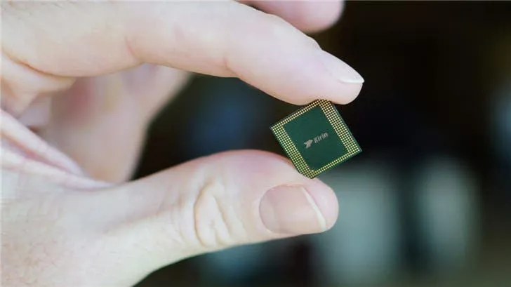
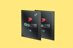
Recently, the vice president of Huawei's mobile phone product line, Bruce Lee, talked about the EUV lithography process used by Kirin 990 5G. According to Bruce Lee, Kirin 990 5G EUV lithography process uses a short wavelength from the previous 193 nm to 10 nm. According to him, this is a major breakthrough in the semiconductor field.

Huawei was able to integrate 10.3 billion transistors in an area of about 200 mm2 which is almost half that of the previous generation. However, what exactly is EUV? It is the abbreviation for Extreme Ultraviolet Lithography. Often called EUV lithography, it has a wavelength of 10-14 nm. It is also a lithography technique which uses extreme ultraviolet light.
Huawei Kirin 990 5G uses TSMC's 7nm+ EUV process. According to reports, Apple's A13 will also use TSMCs 7nm+ process. In addition, TSMC also revealed that it is steadily advancing the next-generation 5nm process. This process fully applies EUV technology and has begun trial production. The company expects to commence mass production in the first quarter of 2020. Furthermore, TSMC also has a transitional 6nm process which improves on the 7nm process. The 6nm process will also go into trial production in the first quarter of 2020.
Popular News
Latest News
Loading