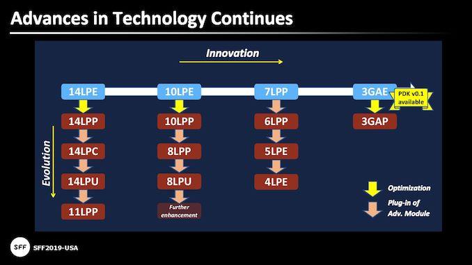
According to TSMC, its capital expenditure in 2020 will be $15 to 16 billion. It will invest 80% of this sum in advanced capacity expansion, including 7nm, 5nm, and 3nm. The company will have a special press conference in April where it will disclose the details of the 3nm process. What route TSMC’s 3nm process technology ultimately chooses is very important to the semiconductor industry. As of now, only TSMC and Samsung have the capacity to work on the 3nm node. Samsung announced the 3nm process last year and will give up FinFET transistors for GAA surround-gate transistor technology.

Specifically, Samsung’s 3nm process is divided into 3GAE and 3GAP, the latter has better performance. According to the official statement, based on the new GAA transistor structure, Samsung has manufactured MBCFETs (Multi-Bridge-Channel FETs) by using nanochip devices. This technology can significantly enhance transistor performance, mainly replacing FinFET transistors technology. In addition, MBCFET technology can also be compatible with existing FinFET manufacturing process technologies and equipment. This will accelerate the process development and production.
At the Japan SFF conference in 2019, Samsung also announced specific specifications for the 3nm process. Compared with the current 7nm process, the 3nm process can reduce the core area by 45%, reduce power consumption by 50%, and improve performance by 35%.

Samsung plans to invest $116 billion to build a semiconductor ecosystem by 2030. Since it is behind TSMC at 7nm and 5nm nodes, Samsung bets on the 3nm node and hopes to surpass TSMC to become the largest wafer foundry at this node. Therefore, Samsung has high hopes for the 3GAE process, and mass production will be as soon as 2021.
As for TSMC, it will also heavily invest in the 3nm node. Last year, it announced that it has invested $19.5 billion in the construction of a 3nm factory and will officially start construction in 2020. However, the technical details are still under wraps. TSMC has the option to choose GAA transistors like Samsung or continue to improve FinFET transistors. These two technological routes will affect the choice of many high-end chips in the future.


