Samsung has announced the availability of its HybridSubstrate Cube dubbed the H-Cube earlier today, November 11. This is the South Korean tech company's latest 2.5D semiconductor packaging option. Moreover, it is exclusively designed for data center requirements, networking, AI products, and HPC which demands large-scale packaging technology. SEMCO (Samsung ElectroMechanics) collaborated with Amkor Technology to develop the H-Cube solution.
The H-Cube solution is a great choice for high-performance semiconductors that require the integration of multiple chips, according to Moonsoo Kang. Kang is the senior vice president and head of Samsung's Foundry Business Model Team. Moreover, Kang assures that Samsung will be supplying several packaging options in a bid to resolve issues the company's clients face. The company will need to expand and enhance its foundry ecosystem to achieve this, Kang added.
Samsung Announces H-Cube Solution
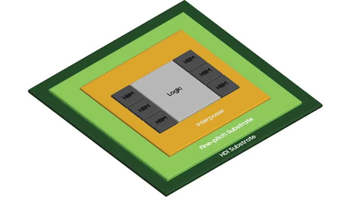
The 5D package comes in a compact form factor, allowing users to install HBM (high bandwidth memory) or logic chips above silicon supplements. The Samsung H-Cube system features a hybrid platform, coupled with a fine pitch platform that can fine bump connections and is capable of HDI (high-density interconnection). This allows massive sizes to fit inside a 2.5D packaging. Aside from that, large-area packaging becomes more important as the quantity and size of chips inside a package increases.

Furthermore, it is important to have high-speed broadband communication. Also, fine-pitch substrates are important but the prices increase as the size increases, according to a blog post on Samsung Newsroom. If six or more HBMs are put together, it is harder to create a huge substrate. As a result, the efficiency reduces. The Korean tech behemoth solved this problem with the help of a hybrid substrate structure, which forms a combination of easily processable HDI substrates and a high-end fine-pitch platform over a massive expanse.
Other Vital Information
When the solder ball pitch reduces by 35 percent, the fine-pitched platform's size is likely to reduce. The solder ball pitch electrically links the platform and the chip. Meanwhile, an HDI substrate (PCB module) can come under the fine pitch substrate get interaction with the board system. Aside from that, the H-Cube solution's dependability can increase by employing Samsung's power and signal integrity analysis technology. This technology helps deliver steady power without causing distortion or signal loss while piling up multiple HBM and logical chips.
Aside from improving the H-Cube solution's reliability, Samsung's proprietary signal/power integrity analysis technology assures a stable supply of power. Samsung is currently gearing up to hold its third SAFE (Annual ‘Samsung Advanced Foundry Ecosystem) Forum. The event will kick off virtually on November 17 (PST).
Popular News
Latest News
Loading