Samsung’s 2nd-Gen 3nm process, SF3, has begun trial production
SamsungSunday, 21 January 2024 at 15:52
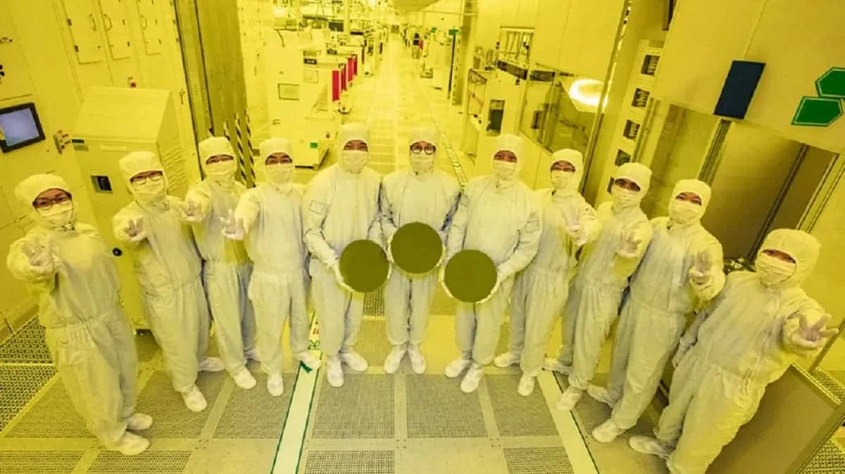
Samsung Foundry has reportedly begun trial production of chips on its 2nd Generation 3nm-class process technology, known as SF3. This development marks a significant milestone in the semiconductor industry, as Samsung competes with TSMC for supremacy in the upcoming mass production of advanced process nodes. According to Chosun Ilbo, a popular and authoritative news outlet in South Korea, Samsung is now producing the 2nd-Gen 3nm process chip, SF3 on trial. The report claims that Samsung expects to hit yield rates of over 60% within the next six months.

Digitimes reported that Samsung is testing the performance and reliability of chips manufactured on the SF3 node. This is the first chip using Samsung's SF3 process and is expected to be an application processor designed for wearable devices. Most likely, the company will release this chip just in time for the Samsung Galaxy Watch 7 and other devices.
SF3 Process: A Breakthrough in Semiconductor Technology
The SF3 process is a 3nm-class technology that builds upon Samsung's first-generation 3nm process. This new process is expected to lead the AI era, as it will enable the production of more efficient and powerful chips. The trial production of SF3 chips is a crucial step towards the full ramp of the SF3 node. After the trial production, the company will commence the full-scale production probably later this year. Chosun Ilbo says it expects Samsung to also use this node for the Exynos 2500 chip. The Exynos 2500 will likely launch with next year's Samsung Galaxy S25 series.
Samsung has previously stated that it plans to start large-scale mass production of SF3 chips in the second half of this year. The company will focus on the production of its 3nm chip SF3 (3GAP) and its better version SF3P (3GAP+) this year. As for the 2nm node, Samsung has since confirmed that it will roll out its plans in two years.
According to Samsung, the SF3 node can enable different gate-all-around (GAA) transistor nanosheet channel widths within the same cell, providing greater design flexibility. This can also bring lower power consumption and higher performance to the chip, and increase transistor density through optimized design.

Impact of SF3 on the Semiconductor Industry
The SF3 process is expected to have a significant impact on the semiconductor industry. It will enable the production of more efficient and powerful chips. This will lead to advancements in various sectors, including AI, IoT, and automotive. This chip also has the potential to revolutionize semiconductor performance and power consumption. Some key aspects of SF3's impact include:
1. Wider range of applications: SF3 technology is expected to be adopted in a wider range of applications, making GAA nanosheets more versatile and suitable for various chip designs.
2. Increased versatility**: SF3 technology is designed to enhance the performance and power efficiency of data center CPUs and GPUs, providing a competitive edge over other foundries.
3. Advanced packaging technology: SF3 technology is compatible with advanced packaging technologies, which can contribute to enhanced transistor density and power efficiency.
4. Competitive edge: Samsung's SF3 technology is expected to be the first to market with GAA FETs, which control current leakage better than finFETs at the most advanced nodes. This competitive edge can help Samsung maintain its position in the semiconductor industry.
5. Follow-on technologies: Samsung is also working on follow-on technologies, such as SF4E, 4, and 4P, which are expected to be introduced in the mobile market. These technologies can further enhance Samsung's position in the semiconductor industry.
The Future of Samsung's Semiconductor Business
Samsung's investment in the development of the SF3 process demonstrates the company's commitment to innovation and its ambition to lead the AI era. The successful trial production of SF3 chips is a testament to Samsung's expertise in semiconductor technology and its ability to stay ahead of the competition. As the full ramp of the SF3 node approaches, Samsung is poised to make a significant impact on the semiconductor industry and contribute to the growth of the AI era.

The company's semiconductor business is expected to continue growing in the future. Samsung is investing heavily in research and development, as well as expanding its manufacturing capacity. Last year, Samsung's semiconductor technologies pushed the boundaries in AI, HPC, and connectivity. The company is also steering its semiconductor partners through a new era of growth. Samsung Electronics expects to invest $230 billion over the next 20 years to develop its chipmaking base in South Korea. This is in line with efforts to boost the national chip industry.
Samsung is one of only three companies that manufacture the world's most advanced chips. It ranks second behind TSMC and ahead of Intel. The company is also setting its sights on catching TSMC. It announced an ambitious new roadmap, pursuing a goal to triple the capacity of leading-edge manufacturing.
Final Words
Samsung's 2nd-Gen 3nm process, SF3, has begun trial production, marking a significant milestone in the semiconductor industry. This development will lead to the production of more efficient and powerful chips. These chips will also contribute to advancements in various sectors and solidify Samsung's position in the market. The full ramp of the SF3 node is set to come later this year. It will further solidify Samsung's position in the AI era and demonstrate the company's commitment to innovation and growth.
Author Bio
Efe Udin is a seasoned tech writer with over seven years of experience. He covers a wide range of topics in the tech industry from industry politics to mobile phone performance. From mobile phones to tablets, Efe has also kept a keen eye on the latest advancements and trends. He provides insightful analysis and reviews to inform and educate readers. Efe is very passionate about tech and covers interesting stories as well as offers solutions where possible.
Popular News


Latest News
Loading