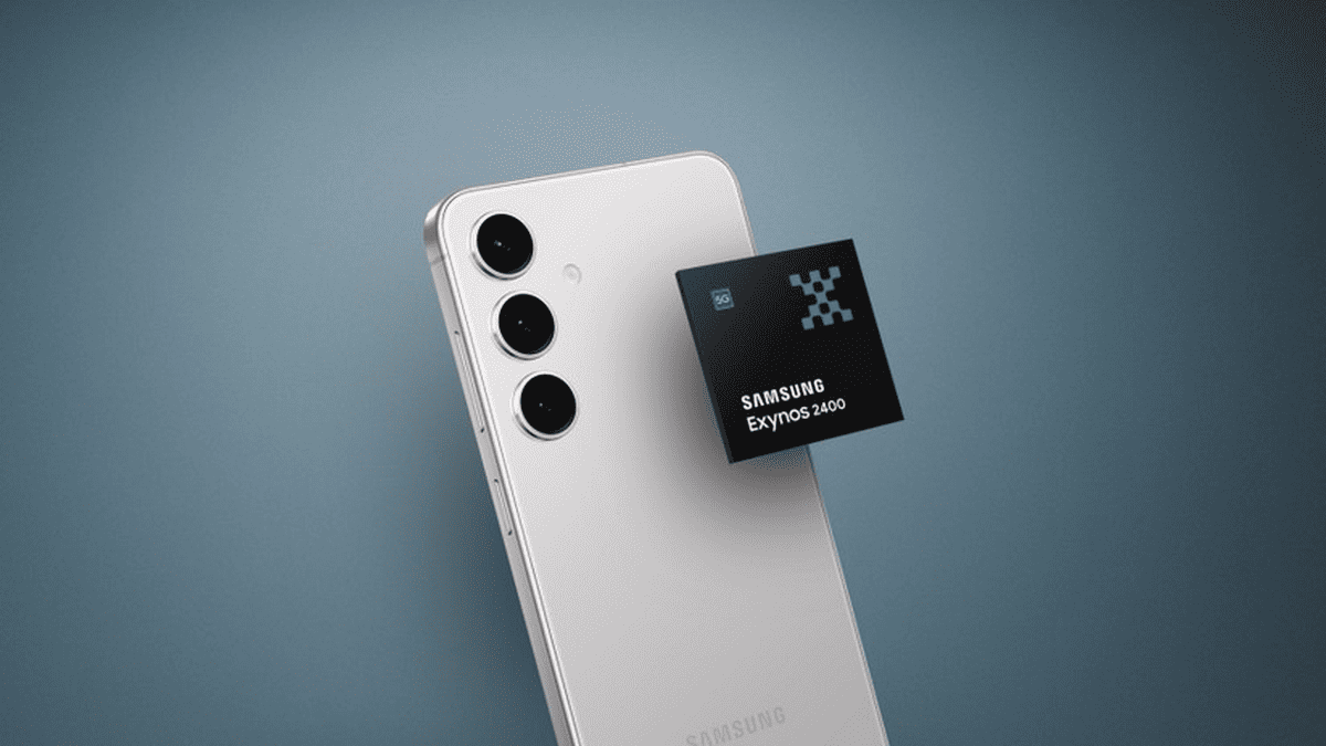
According to popular and authoritative tech blogger, @Tech_Reve, Samsung Exynos 2400 currently has a yield rate of about 60%. This shows that the 4LPP+ is quite stable relative to other processes. Although it is not as good as competitors (TSMC N4P is said to be about 70%), it has been far better than the one of last year. The Exynos 2400 is Samsung’s first smartphone chipset to adopt “fan-out wafer-level packaging” (FOWLP). Samsung claims that using FOWLP technology can increase heat resistance by 23%, resulting in an 8% improvement in multi-core performance. This is why the Exynos 2400 performs well in the latest 3DMark Wild Life extreme stress test results. Last month, Chosun said that Samsung Electronics foundry has started trial production for its second-generation 3nm process SF3. The company reportedly plans to increase yield rates to over 60% within the next six months.

What is the Yield Rate?
The semiconductor yield is the percentage of the total number of chips produced to the maximum chip count on one wafer. Simply put, it refers to the proportion of defect-free chips produced in the manufacturing process. This directly impacts production costs, product quality, and overall profitability.
For instance, Samsung’s yield rate for the 4 nm technology was reported to be around 50%. These figures indicate the challenges and fluctuations in chip yield rates that Samsung has experienced in recent years. Despite the setbacks, Samsung invested heavily in research and development, process refinement, and advanced manufacturing technologies to address yield rate issues. It appears that the company’s investment is now paying off as its yield rate is now improving.
The yield rates of semiconductor chips are influenced by various factors such as manufacturing processes, technological advancements, and production techniques. Companies like Samsung continuously work to improve their yield rates through research, development, and innovation. It’s important to note that yield rates can significantly impact the overall production and profitability of a semiconductor manufacturer.
Exynos 2400 Manufacturing Process
The Exynos 2400 is manufactured using Samsung Foundry’s second-generation 4nm process (4LPP), which is a low-power process optimized for performance and power efficiency. Also, Samsung has started using Fan-Out Wafer Level Packaging (FOWLP) for the Exynos 2400, which makes the chip smaller, thinner, and more power-efficient. This manufacturing process and packaging technology are expected to contribute to the performance and power efficiency of the Exynos 2400 chip.

According to reports, Samsung is also testing the performance and reliability of chips manufactured on the SF3 node. The first chip to use Samsung’s SF3 process is expected to be an application processor designed for wearable devices. This chip will probably launch with the Galaxy Watch 7 later this year.
Samsung has previously stated that it plans to start large-scale mass production of SF3 chips in the second half of 2024. 2023-2024 will be dominated by 3nm production, namely SF3 (3GAP) and its improved version SF3P (3GAP+). The company also plans to -start rolling out its 2nm node in 2026. According to Samsung, the SF3 node can enable different gate-all-around (GAA) transistor nanosheet channel widths within the same cell, providing greater design flexibility. This can also bring lower power consumption and higher performance to the chip, and increase transistor density through optimized design.
Even with all of these, Samsung is still behind TSMC. According to TrendForce data, TSMC accounted for 57.9% of the global foundry market in the third quarter of last year. Samsung Electronics ranked second with a 12.4% share, with a gap of more than 40 percentage points between the two companies.
Exynos 2400 Features
Samsung’s Exynos 2400 is constructed using an improved version of Samsung Foundry’s 4nm fabrication process, which now boasts a 60% yield rate. The Exynos 2400 is a 10-core CPU configuration that includes a high-performance Cortex-X4 core clocked at 3.1GHz, two Cortex-A720 cores clocked at 2.9GHz, three Cortex-A720 cores clocked at 2.6GHz, and four Cortex-A520 cores clocked at 1.8GHz. The Exynos 2400’s CPU performance is 70% faster than the Exynos 2200, and its AI processing power is 14.7 times faster. Its 2400’s GPU has been co-designed with AMD, promising exceptional graphics capabilities.
Conclusion
Samsung’s semiconductor journey, marked by fluctuations in chip yield rates, showcases the dynamic nature of the technology industry. The recent improvements in yield rates, particularly with the Exynos 2400 chip utilizing the 4LPP+ process, underscore Samsung’s commitment to innovation and operational excellence. The Exynos 2400’s utilization of “fan-out wafer-level packaging” (FOWLP) is a testament to the company’s focus.
Understanding the significance of yield rates in semiconductor production is crucial. It reflects the proportion of defect-free chips, impacting production costs, product quality, and overall profitability. Samsung’s investment in research, development, and advanced manufacturing technologies has been instrumental in addressing yield rate issues. The company is now driving improvements in production efficiency and product quality.
While Samsung continues to make significant strides, it faces fierce competition, particularly from TSMC. The emergence of advanced nodes like SF3 and SF3P underscores Samsung’s ongoing efforts. The company wants to remain competitive and innovative in the semiconductor landscape. The company is moving forward with its semiconductor roadmap. The roadmap includes plans for large-scale mass production of SF3 chips and the rollout of its 2nm node. The company is also focused on delivering cutting-edge solutions that drive technological innovation and shape the future of the industry.
Author Bio
Efe Udin is a seasoned tech writer with over seven years of experience. He covers a wide range of topics in the tech industry from industry politics to mobile phone performance. From mobile phones to tablets, Efe has also kept a keen eye on the latest advancements and trends. He provides insightful analysis and reviews to inform and educate readers. Efe is very passionate about tech and covers interesting stories as well as offers solutions where possible.


