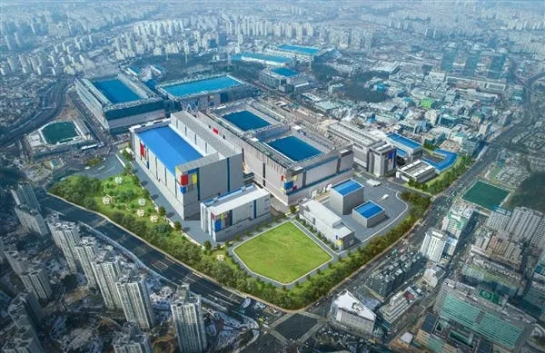
Samsung is expanding its production capacity of 7-nm EUVs by investing $6 Billion in a new semiconductor plant in Hwaseong, Korea. This announcement was made today after Samsung reached an agreement with Qualcomm to produce future 5G mobile device chips which will be based on Samsung's 7nm LPP manufacturing process and the technology node will introduce EUV (EUV lithography).

According to the construction schedule, this plant should be ready by the second half of 2019 and full-scale production should commence by 2020. As stated earlier, the production will make use of EUV (extreme ultraviolet) lithography which in theory should give Samsung’s 7nm chips technological superiority over 7nm chips from its major rival TSMC.
As of now, Samsung has a total of four semiconductor plants globally. Two are located in South Korea (Giheung and Pyeongtaek) while the other two are abroad (Austin, Texas and Xi'an, China). In 2017, Samsung investment in the semiconductor business reached $26 Billion, setting a record high, mainly due to the huge demand for its memory chips.
Bron: sammobile
Popular News


Latest News
Loading