
In recent times, TSMC and Samsung have made great progress in the chip manufacturing industry while Intel lags behind. In addition to technological breakthroughs, TSMC and Samsung have adopted more flexible tactics, reduced the difficulty of new technology, and made a new version as soon as possible.

For example, TSMC's 16nm is an important node, and the 12nm process is an upgraded and optimized version of the 16nm process. Recently, TSMC announced that the 5nm EUV process has begun trial production. Compared with 7nm, the core area can be reduced by 45% and the performance can be increased by 15%. At the same time, the Samsung 5nm EUV process has been designed to reduce power consumption by 20% compared with 7nm and the performance is increased by 10%.
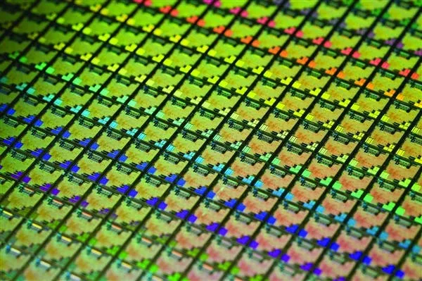
Now, TSMC has officially announced the 6nm (N6) process, which has been greatly enhanced on the basis of the existing 7nm (N7) process. It is said to be highly competitive and cost-effective and can accelerate product development, and mass production.
The new 6nm process also uses EUV lithography, which claims to increase transistor density by 18% compared to the 7nm process, while the design rules are fully compatible with the 7nm process which facilitates upgrade migration and lowering costs. TSMC's 6nm process is expected to be trial production in the first quarter of 2020 and it will be suitable for mid- to high-end mobile chips, consumer applications, AI, network, 5G, and high-performance computing.
Popular News


Latest News
Loading