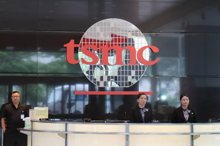
According to recent reports, TSMC has quietly introduced a performance-enhancing version of the 7nm deep-UV DUV (N7) and 5nm EUV E-UV (N5) manufacturing processes. The company's N7P and N5P technologies are for customers who need a 7nm design to run faster or consume less power.

TSMC's new N7P process uses the same design rules as the N7 to optimize front-end (FEOL) and mid-range (MOL). This can increase performance by 7% at the same power or 10% at the same frequency. TSMC first disclosed relevant information at the VLSI seminar held in Japan this year. However, there was no wide publicity to this improvement. The N7P uses proven deep ultraviolet (DUV) lithography to reduce transistor density compared to N7.
TSMC customers who require transistor density higher than approximately 18% to 20% will probably use the N7+N6 process technology. Among them, the N6 process technology is multi-layered by ultra-violet (EUV) lithography. In addition, TSMC's next major node is the N5 (5nm). This comes with significant density, lower power consumption, and higher performance. It will also have a performance-enhancing version called N5P. The technology uses FEOL and MOL optimization to increase the chip's operating speed by 7% at the same power or 15% at the same frequency.
Popular News


Latest News
Loading