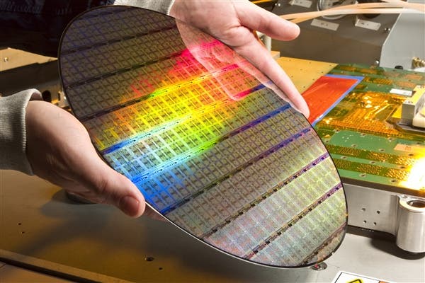
According to recent reports, TSMC’s 6nm process technology will enter trial production in the first quarter of next year. TSMC also confirmed that the 6nm manufacturing process will enter mass production by the end of next year. The company said its 7nm high-performance (N7+) process with ultra-violet (EUV) lithography has helped its customers. The N7+ (with EUV lithography), is based on its successful 7nm process. This process lays the foundation for the 6nm process.

The mass production rate of N7+ is one of the fastest in history. It started mass production in the second quarter of 2019. N7+ also provides an overall performance boost. N7+’s logic density is 15% to 20% higher than N7 while reducing power consumption. TSMC quickly increased its capacity to meet the needs of multiple customers for N7+.
TSMC said that EUV lithography technology enables the company to continue to push wafer miniaturization because the shorter wavelengths of EUV can better analyze the design of advanced processes. TSMC’s EUV equipment is now mature and can achieve its mass production goals. The output power in daily operation is more than 250 watts.
TSMC said that the successful completion of N7+ is the cornerstone for future advanced processes. With the further application of EUV lithography, the N6’s logic density will be 18% higher than that of the N7. Furthermore, the N6 design rules are fully compatible with the N7. Thus it can significantly shorten its time-to-market for customers.


