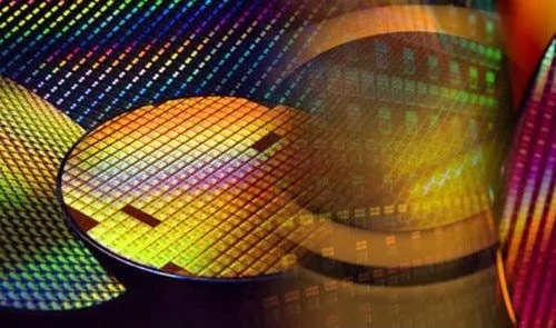
Of course, after the mass production of TSMC's 5nm process, the next generation's major chip process will be 3nm. According to TSMC, the research and development of its 3nm process are proceeding as scheduled. TSMC recently revealed that it will commence risk trial production in 2021. However, large-scale mass production should commence in the second half of 2022. Although we still have nearly two years before TSMC’s 3nm process is put into mass production, many manufacturers are paying attention to TSMC’s advanced process technology.

Reports show that TSMC is preparing four waves of production capacity for the 3nm process. However, most of the production will be for their major customer, Apple. Most of the first wave of TSMC's 3nm process capacity is left to Apple, which is actually expected. Apple is a major customer of TSMC. Starting from the A10 processor in the iPhone 7 series in 2016, Apple’s A-series processors have been exclusively manufactured by TSMC.
The 3nm process is a complete process node leap after 5nm, which will significantly improve the performance of the chip. At the company's financial report meetings in the first and second quarters of this year, TSMC CEO, Wei Zhejia, revealed that compared with the 5nm process, the 3nm process will increase the density of transistors by 70% and the speed of the chip by 10% - 15%. The energy efficiency will also increase by 25% to 30%.
TSMC is already working on its 2nm process
According to the Taiwan Economic Daily, TSMC’s 2nm process has made a major breakthrough. The research and development process is now in advanced stages. The company is optimistic that its risk trial production yield in the second half of 2023 can reach 90%. The supply chain also revealed that unlike 3nm and 5nm processes that use FinFET, TSMC 2nm process uses a new multi-bridge channel field effect transistor (MBCFET) architecture.
TSMC established a 2nm project R&D team last year to find a feasible path for development. Considering cost, equipment compatibility, technology maturity, and performance, 2nm adopts the MBCFET architecture based on the surround gate (GAA) process. This solves the physical limit of FinFET’s current control leakage due to process shrinkage. TSMC previously revealed that its 2nm R&D and production will be in Baoshan and Hsinchu. It is also planning for four ultra-large wafer fabs from P1 to P4, covering an area of more than 90 hectares.
Looking at the current R&D progress of TSMC’s 2nm, it should enter risk trial production in 2023 and mass production in 2024.
Popular News

Latest News
Loading