Samsung and IBM chip design promises one-week battery life for smartphones
SamsungMonday, 13 December 2021 at 21:09
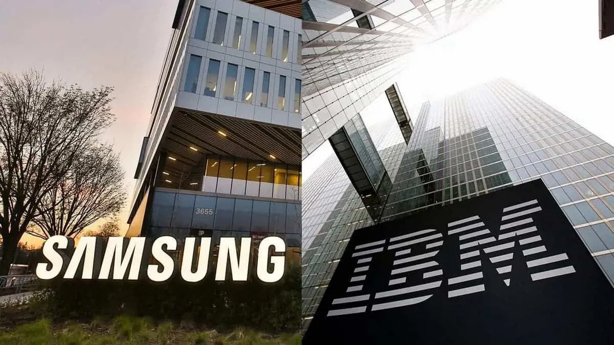
Samsung and International Business Machines (IBM) has launched during the IEDM conference in San Francisco a new design for stacking transistors. One of the companies behind the rise of computing, and the largest smartphone maker, and also one of the biggest chip manufacture and general electronics maker have joined forces. The new semiconductor design will be achieved by stacking transistors vertically on a chip.
The new architecture bears Vertical Transport Field Effect Transistors (VTFET), transistors sit perpendicular to one another and the current flows through them vertically. For those who are unaware, in the current processors and system on chips, the transistors lie flat on the surface. The electric current flows from side to side. This new kind of transistor will allow for a greater density of these components per chip compared to anything that is available at present. Therefore, there's potential for improved power efficiency or performance.
Samsung and IBM want to extend Moor's Law beyond the nanosheet threshold and waste less energy in the process. The two giants say that it will double the performance or use 85 percent less power than chips that use the current FinFET transistors.

The companies are among the first to disclose the new technology. However, they aren't the only ones. Another giant in the chip industry, Intel, is also working on chips stacked above each other to save area. Intel's goal is also to reduce interconnect lengths and save energy to make the chips more cost-efficient and better performing. Intel aims to finalize the design for angstrom-scale chips by 2024. It will appear in the company's "Intel 20A" node and RibbonFET transistors.
The new design promises one-week battery life for smartphones and power-efficient crypto-mining
Interestingly, IBM and Samsung are making bold claims when it comes to the benefits of such technology. According to the companies, the new standard may one day allow smartphones to go a full week on a single charge. That's really impressive in a world where we need to charge super-expensive smartphones on a daily basis. The company also says that it could make certain energy-intensive tasks, including crypto mining, more power-efficient. Therefore, they would be less impactful on the environment.
Unfortunately, IBM and Samsung didn't say when the design will go commercial. However, we assume that still is a couple of years away from becoming a reality. After all, we've just reached the 4 nanometers node. We still expect companies to try 3nm and 1nm before breaking the barrier.
Popular News


Latest News
Loading