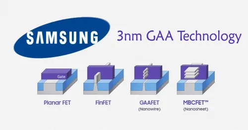
Samsung reveals in the latest briefing to investors that its 3nm process will start production in the next few weeks. If this comes to fruition, its progress is faster than TSMC. However, TSMC never comments on its competitors. According to TSMC, the 3nm with FinFET architecture will enter mass production in the second half of the year. Industry analysts believe that although Samsung claims that 3nm is entering the countdown to mass production, from the perspective of transistor density and performance, Samsung's 3nm is comparable to TSMC's 5nm and Intel's Intel 4nm process.

Samsung's "3nm" process is the latest theoretically but practically, it still lags behind TSMC. Samsung briefed investors that it is fully preparing to put the GAA-based 3nm process into production in the first half of this year. This means that it will start the mass production process in the next eight weeks.
Samsung claims that relative to its current 7nm FinFET architecture process, the new 3nm process chips can work in a low-voltage environment below 0.75 volts. This will reduce the overall power consumption by 50%. It will also improve the performance by 30%, and reduce the chip size by 45%.
Although Samsung's 3nm process will be comparable to TSMC's 4nm process, the former's bandwidth and leakage control performance will be better. This will most likely result in better performance.
Samsung's 3nm process yield rate remains unknown
However, the biggest variable that cannot be known at present is how good Samsung's 3nm process yield can be. Samsung's 4nm process has a really low yield rate and this is causing major customers to switch to TSMC. According to industry reports, Samsung's 3nm yield rate is only about 10%, but it has not been confirmed by Samsung.
The industry believes that major manufacturers such as Apple, AMD, NVIDIA, Qualcomm, Intel, and MediaTek will be the main customers of TSMC in the early stage of 3nm mass production, with applications covering high-speed computing, smartphones and other fields. TSMC claims that after the mass production of 3nm in the second half of this year, it will lead in PPA (performance, power consumption and area) and transistor technology. It will also have a good yield rate. It is confident that 3nm will continue to win the trust of customers.
In addition, TSMC has also embarked on a more advanced 2nm layout. It is expected to start risk trial production in 2024 and target mass production in 2025. It is optimistic that 2nm will be the industry's leading technology and the most suitable technology to support customer growth.
Popular News
Latest News
Loading


