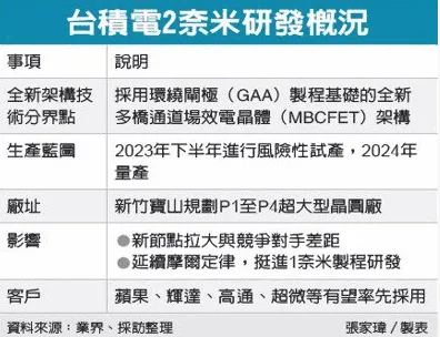
According to the Taiwan Economic Daily, TSMC’s 2nm process has made a major breakthrough. The research and development process is now in advanced stages. The company is optimistic that its risk trial production yield in the second half of 2023 can reach 90%. The supply chain also revealed that unlike 3nm and 5nm processes that use FinFET, TSMC 2nm process uses a new multi-bridge channel field effect transistor (MBCFET) architecture.

TSMC established a 2nm project R&D team last year to find a feasible path for development. Considering cost, equipment compatibility, technology maturity, and performance, 2nm adopts the MBCFET architecture based on the surround gate (GAA) process. This solves the physical limit of FinFET's current control leakage due to process shrinkage. TSMC previously revealed that its 2nm R&D and production will be in Baoshan and Hsinchu. It is also planning for four ultra-large wafer fabs from P1 to P4, covering an area of more than 90 hectares.
Looking at the current R&D progress of TSMC's 2nm, it should enter risk trial production in 2023 and mass production in 2024
Transistors - a key to advanced semiconductor manufacturing processes
Transistors are the key to breakthrough advanced semiconductor manufacturing processes. For example, at the 45nm stage, the industry introduced the high-k insulating layer/metal gate (HKMG) process. The second-generation high-k insulating layer/metal gate process was introduced at 32nm. However, when the size of the transistor is less than 25nm, the size of the traditional planar field effect tube cannot be reduced.

The Fin Field-Effect Transistor (FinFET) invented by Professor Hu Zhengming of the University of California at Berkeley solves this problem. The main idea is to make the field-effect transistor three-dimensional. This new complementary metal oxide semiconductor transistor can improve circuit control and reduce leakage current.
Thanks to the invention of FinFET, Intel launched a commercial 22nm FinFET in 2011. Since then, the FinFET industry has advanced the semiconductor manufacturing process from 22nm to 5nm today. However, the 5nm process has reduced the transistor to the atomic level. The diameter of silicon atoms is 0.117nm, and 3nm is almost the length of 25 silicon atoms connected end to end.
FinFET technology will stop at 4nm/3nm manufacturing process
To continue the process of miniaturizing semiconductors, new technologies need to be introduced. The GAA (Gate-all-around, around the gate) adopted by TSMC 2nm is also called GAAFET. It has the same concept as FinFETs. The difference is that the gate of GAA wraps around the channel. According to different designs, GAA also has different forms. The current four mainstream technologies are nanowires, sheet-like structure multi-way bridging fins, hexagonal cross-section nanowires, and nanorings.

The GAA technology introduced by Samsung is Multi-Bridge Channel FET (MBCFET), which is a multi-channel bridge fin with a plate-like structure. In the adoption of GAA technology, Samsung is even more radical. It is reported that Samsung 3nm will introduce GAA to increase its 3nm process performance by 35% and reduce power consumption by 50% compared to 7nm. However, TSMC will not introduce GAA technology until 2nm.
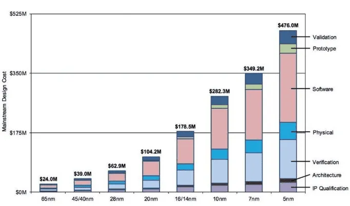
GAA can bring performance and power consumption reduction, but the cost is also very high. The cost of the 28nm process is $62.9 million, and 5nm will surge to $476 million. Samsung claims that the cost of its 3nm GAA may exceed $500 million.
Popular News
Latest News
Loading


