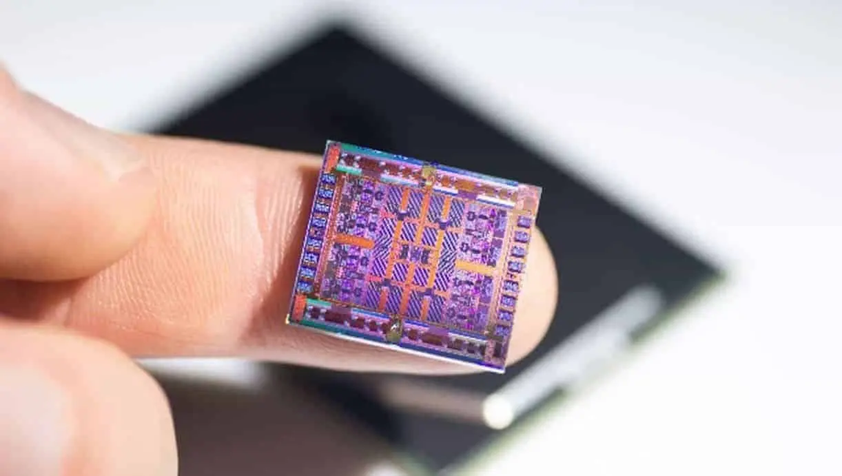
Samsung, a leading semiconductor manufacturer, has recently made waves in the
tech industry by announcing a significant change in its nomenclature for the upcoming second-generation
3nm process. This move involves renaming the process to "2nm," a decision that has sparked discussions and curiosity among industry experts and enthusiasts alike. Samsung already had a 3nm process. However, as it advanced its manufacturing process, it initially decided to call it the
2nd Gen 3nm process. Sometime last year, there were reports that the company would change the name of this process. Now, there is official confirmation from Samsung that it will call its new manufacturing process, "2nm". According to Samsung, this process should start mass production before the end of this year.
South Korea's ZDNet reports that Samsung Electronics has notified customers and partners that it will rename the second-generation 3-nanometer process to the 2-nanometer process starting from the beginning of this year. A fabless industry insider said:
"We received notification from Samsung Electronics that they are changing the second-generation 3nm to 2nm. The second-generation 3-nanometer contract we signed with Samsung Electronics foundry last year was also renamed 2-nanometer, so we need to rewrite the contract in the near future."
Samsung 2nm process order and plans
Japanese AI giant Preferred Networks Inc. (PFN) chose Samsung and placed its first
2nm process AI chip production order with it. This 2nm order is actually the "second generation 3nm".
Samsung Electronics became the world's first company to mass-produce 3-nanometer chips based on the all-gate (GAA) process at the end of June 2022. It planned to mass-produce the second-generation 3-nanometer process this year and the 2-nanometer process in 2025.
A semiconductor industry insider said:
Samsung Electronics' second-generation 3nm (2nm) process design kit (PDK) has been released, so if Samsung rushes into mass production this year, they will be well-positioned to do so. As for the specific mass production time, it depends largely on customer requirements.
According to industry insiders, Samsung Electronics' change of process name may be beneficial to OEM marketing. This is also the recent public relations trend in the foundry industry.
When Samsung Electronics shifted from the 7-nanometer process to the 5-nanometer process in 2020, the second-generation 7-nanometer process was renamed the 5-nanometer process. Samsung Electronics' 7-nanometer process became the world's first process to use extreme ultraviolet (EUV)
technology in 2019. This makes it more stable and allows the company to shrink transistor sizes. This is why the second generation of 7nm was renamed 5nm.
Industry insiders said:
The second generation of 3nm reduces the transistor size, on the one hand for marketing or publicity needs, and on the other hand it can also be seen as one of the results of advancement work
The Evolution of Semiconductor Technology
Semiconductor technology has been advancing at a rapid pace, driving innovation across various sectors such as computing, telecommunications, and consumer electronics. The transition from larger process nodes to smaller ones has been a key trend in the industry, enabling manufacturers to pack more transistors into a given area, thereby improving performance and energy efficiency.
Samsung's Technological Milestones
Samsung has been at the forefront of semiconductor innovation, consistently pushing the boundaries of what is possible in chip manufacturing. The company's first-generation 3nm process marked a significant leap forward in terms of transistor density and power efficiency. By announcing the renaming of the second-generation 3nm process to "2nm," Samsung is signalling another milestone in its technological journey.
Implications of the Renaming
The decision to rename the second-generation 3nm process to "2nm" carries several implications for both Samsung and the semiconductor industry as a whole. One immediate impact is on marketing and branding – by simplifying the nomenclature, Samsung aims to create a clearer and more intuitive naming convention for its products. This could potentially enhance consumer understanding and perception of the technology.
Technological Advancements in the 2nm Process
Beyond the name change, what truly matters are the technological advancements that Samsung's 2nm process will bring. With each successive generation of semiconductor technology, manufacturers strive to achieve higher transistor density, lower power consumption, and improved performance. The 2nm process is expected to deliver on these fronts, opening up new possibilities for next-generation devices.
Competition in the Semiconductor Industry
Samsung operates in a highly competitive landscape alongside other major players such as TSMC and Intel. The renaming of its second-generation 3nm process to "2nm" can be seen as a strategic move to stay ahead in this competitive race. By aligning its naming convention with industry standards and expectations, Samsung aims to maintain its position as a leader in
semiconductor manufacturing.
Future Prospects and Industry Trends
Looking ahead, the semiconductor industry shows no signs of slowing down. As demand for more powerful and energy-efficient chips continues to rise, manufacturers like Samsung will play a crucial role in shaping the future of technology. The renaming of the second-generation 3nm process to "2nm" is just one example of how companies are adapting to meet these evolving demands.
Conclusion
In conclusion, Samsung's decision to rename its second-generation 3nm process to "2nm" reflects a shift in terminology. It also reflects a deeper commitment to innovation and progress. The need for the change could be for marketing purposes. It could also help Samsung to be the first company to mass produce the 2nm process. As we move towards the future, advancements in semiconductor manufacturing will be key drivers of this transformation. Samsung's rebranding is not just about numbers; it symbolizes a continued journey towards smaller, faster, and more efficient chips that will power the devices of tomorrow. Through this strategic move, Samsung reaffirms its position as a pioneer in semiconductor technology and sets the stage for further breakthroughs in the years to come.